The landscape of artificial intelligence hardware is undergoing a seismic shift, and at the epicenter of this transformation lies a critical component that most consumers will never see: High Bandwidth Memory. As the industry transitions to the fourth generation of this specialized technology, known as HBM4, the ability to manufacture these complex chips with high efficiency is doing more than just determining supply chains it is actively redrawing the lines of leadership among the world’s semiconductor giants. The race to power NVIDIA’s next-generation AI accelerators has become a high-stakes referendum on technological prowess, manufacturing discipline, and strategic foresight, where the difference between market dominance and obsolescence is measured in single-digit yield percentages.
The Critical Role of HBM4 in Next-Generation AI
To understand why HBM4 has become the battleground for semiconductor supremacy, one must first appreciate its role in modern computing. High Bandwidth Memory is not merely a storage component; it is the high-speed data conduit that feeds the insatiable appetite of AI accelerators. As large language models and complex neural networks grow exponentially, the bandwidth between memory and processor has become the primary bottleneck in system performance. HBM4 represents a quantum leap forward, offering data transfer speeds that eclipse its predecessors and enabling the next generation of AI chips to perform trillions of calculations per second without waiting for data .
NVIDIA, the dominant force in AI computing, has built its forthcoming “Vera Rubin” platform around HBM4. This next-generation AI system, particularly the flagship VR200 NVL72 rack solution scheduled for late 2026 delivery, demands memory performance that pushes the boundaries of current manufacturing capabilities . The company has set ambitious specifications, initially targeting data transfer speeds exceeding 11 gigabits per second and ultimately achieving system bandwidth requirements of 22 terabytes per second a nearly seventy percent increase from early design targets . These aggressive performance goals have transformed the supplier selection process from a simple procurement decision into a rigorous technical qualification that few can pass.
The Yield Imperative: Why Manufacturing Efficiency Matters
In the semiconductor industry, “yield” refers to the percentage of functional chips on a silicon wafer that meet performance specifications. This metric is not merely an operational concern; it is the fundamental determinant of profitability, supply capacity, and competitive viability. When yields are low, costs skyrocket, production volumes plummet, and customers face supply uncertainty. In the context of HBM4, yields have become the decisive factor separating market leaders from also-rans.
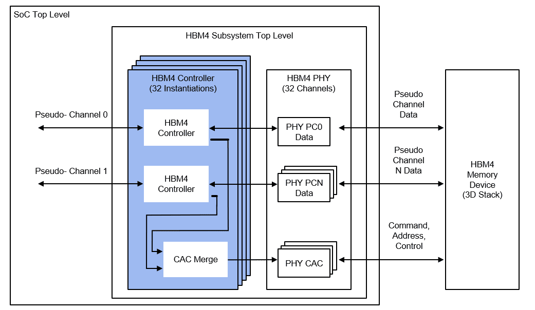
The complexity of HBM4 manufacturing amplifies the importance of yield at every stage. These components are not simple memory chips but sophisticated three-dimensional structures that stack multiple DRAM dies vertically, connected through thousands of tiny electrical paths. The base of each stack includes a logic die essentially a specialized processor that manages data flow adding another layer of manufacturing complexity . With each step in this intricate process presenting opportunities for defects, achieving acceptable yields requires mastery across multiple domains: DRAM fabrication, logic chip manufacturing, advanced packaging, and thermal management.
Micron’s Exit: When Specifications Exceed Capabilities
The most dramatic illustration of yield-driven market restructuring comes from Micron Technology, the third-largest memory manufacturer globally. Initially projected to capture a modest but meaningful share of NVIDIA’s HBM4 business, Micron has been completely excluded from the Vera Rubin supply chain, with its expected market share reduced to zero percent .
This exclusion stems directly from NVIDIA’s decision to raise performance requirements. In the third quarter of 2025, NVIDIA informed potential suppliers that HBM4 must achieve data transfer speeds exceeding 11 gigabits per second . While Micron publicly announced it had reached this threshold, industry sources and supply chain analysts at SemiAnalysis indicate the company struggled to meet the standard with sufficient yields to support volume production . For NVIDIA, which requires millions of units to support its Rubin platform launch, laboratory demonstrations of speed are meaningless without the manufacturing capacity to deliver consistent quality at scale.
The harsh reality facing Micron illustrates a fundamental principle of the AI hardware market: performance specifications are meaningless without manufacturing capability to support them. NVIDIA’s decision to exclude Micron was not based on technical potential but on the practical assessment that the company could not reliably deliver HBM4 meeting the 11.7 gigabits per second target in the volumes required . This left the entire HBM4 market to be divided between Samsung Electronics and SK Hynix, with current estimates suggesting SK Hynix will capture approximately seventy percent of orders while Samsung secures the remaining thirty percent .
Samsung’s Yield Challenges and Strategic Aggression
For Samsung Electronics, the path to HBM4 leadership has been anything but smooth. The company faced significant criticism during the HBM3 generation, when yield problems relegated it to a distant third place in market share, trailing both SK Hynix and Micron . Entering the HBM4 era, Samsung confronted a critical decision: pursue a conservative approach using proven technology to ensure stable supply, or take risks on next-generation processes to leapfrog competitors.
Samsung chose aggression. The company committed to manufacturing its HBM4 using 1c DRAM, the sixth generation of its memory process technology, which offers significant advantages in density, power efficiency, and performance potential . This decision carried substantial risk because 1c yields remained concerning. Reports from late 2025 indicated Samsung’s 1c DRAM yield had not yet exceeded fifty percent in cold testing, below the sixty percent threshold typically required to begin volume production . By comparison, yields for mobile-grade 1c DRAM had reached approximately eighty percent, highlighting the extraordinary difficulty of producing memory capable of HBM4 speeds .
Despite these yield concerns, Samsung made a strategic decision to prioritize speed over perfection. The company considered disbanding its dedicated HBM4 yield improvement task force a team of four to five hundred engineers to accelerate its path to production . Management concluded that securing a position in NVIDIA’s supply chain, even with suboptimal yields, was essential to reversing the company’s declining HBM market share. This gamble appears to be paying off. In February 2026, Samsung announced it had commenced mass production and shipment of HBM4, achieving industry-leading speeds of up to 13 gigabits per second .
Current reports indicate Samsung’s 1c DRAM yield has improved to approximately sixty percent, though when combined with the complex packaging processes required for HBM4, the effective yield declines further . The company’s monthly production capacity for 1c DRAM, estimated at sixty to seventy thousand wafers, remains insufficient to cover NVIDIA’s total HBM4 demand independently, ensuring that SK Hynix will maintain a substantial supply role .
SK Hynix: From Dominance to Structural Vulnerability
If Samsung’s story is one of aggressive risk-taking, SK Hynix’s narrative involves confronting the limitations of past success. Having dominated the HBM3E market with approximately sixty percent share, SK Hynix entered the HBM4 generation with confidence but has encountered unexpected structural challenges .
The most significant vulnerability stems from SK Hynix’s decision to outsource production of the logic die the critical base layer of each HBM4 stack to Taiwan Semiconductor Manufacturing Company . This arrangement, born from SK Hynix’s lack of internal foundry capabilities, creates several complications. First, the company must align its design methodology with TSMC’s process platforms, potentially limiting optimization opportunities. Second, sharing core design data with an external partner raises long-term strategic concerns about intellectual property protection. Third, and most critically, SK Hynix’s production volumes depend entirely on securing sufficient manufacturing capacity from TSMC, which faces overwhelming demand from numerous customers .
This dependency has manifested in practical challenges. During early reliability assessments, SK Hynix encountered difficulties achieving the 11 gigabits per second performance threshold, forcing the company to pursue hardware improvements while the final remained unconfirmed . The reliance on TSMC also limits SK Hynix’s ability to respond quickly to customer requests for customized specifications, as any design change requires coordination with an external partner .
Compounding these foundry challenges is SK Hynix’s conservative DRAM process strategy. Rather than immediately adopting next-generation 1c DRAM for HBM4 production, the company chose to begin with the established 1b process, citing yield stability concerns . While this decision ensured reliable initial production, it creates long-term competitive disadvantages. The 1c process offers superior density and power efficiency, characteristics essential for achieving the ultra-high speeds of 13 gigabits per second and above that NVIDIA demands . Additionally, the smaller die area of 1c DRAM increases the number of chips produced per wafer, potentially creating cost advantages that SK Hynix may struggle to match .
The Foundry Factor: Vertical Integration Versus Specialization
The contrasting approaches of Samsung and SK Hynix highlight a fundamental strategic divergence in the semiconductor industry. Samsung benefits from vertical integration, controlling memory fabrication, logic foundry operations, and advanced packaging internally . This structure enables the company to optimize the interaction between memory dies and the logic base die without coordination challenges, potentially achieving superior performance and faster development cycles.
SK Hynix, by contrast, represents the specialized model, focusing on its core competency in memory while relying on partners for complementary technologies. This approach has served the company well historically, allowing it to concentrate resources on memory innovation. However, HBM4 represents a turning point where the boundaries between memory and logic blur. As academics describe it, this is the “system semiconductorization of memory,” where storage components increasingly perform computational functions . In this new paradigm, control over the logic die becomes as important as memory manufacturing prowess.
The foundry dependency creates particular vulnerability given current geopolitical tensions. SK Hynix’s logic die supply chain relies one hundred percent on TSMC, located in Taiwan amid heightened cross-strait tensions . Any disruption to TSMC’s operations whether from natural disaster, geopolitical conflict, or capacity allocation decisions would directly impact SK Hynix’s ability to deliver HBM4. Samsung, manufacturing its logic dies internally in Korea, faces no comparable supply chain concentration risk.
NVIDIA’s Strategic Response: Pragmatism Over Perfection
Facing supply challenges from both primary suppliers, NVIDIA has demonstrated strategic flexibility in its approach to HBM4 procurement. Rather than rigidly insisting on maximum performance specifications, the company appears willing to accept a tiered approach that balances capability with availability .
According to industry reports, NVIDIA will likely procure both highest-specification HBM4 chips operating at 11.7 gigabits per second alongside slightly lower-performance versions running at 10.6 gigabits per second . This dual-track procurement strategy serves multiple purposes. It relieves pressure on suppliers struggling to achieve maximum speeds at scale, enables both Samsung and SK Hynix to qualify larger portions of their production for NVIDIA’s use, and ensures that Rubin platform launches proceed on schedule even if peak performance components face constraints .
This pragmatic approach reflects NVIDIA’s recognition that supply stability has become as important as raw performance. With memory shortages expected to intensify throughout 2026, ensuring consistent component availability takes precedence over marginal performance gains . For suppliers, this creates an environment where yields matter more than ever not just for profitability, but for the ability to secure and retain customer commitment.
Technical Complexity as Competitive Moat
The HBM4 generation introduces technical requirements that fundamentally alter the competitive landscape. Unlike previous HBM iterations, which primarily demanded advances in memory density and speed, HBM4 requires integration capabilities that few companies possess.
The logic die at the base of each HBM4 stack must now handle increasingly sophisticated functions, managing data flow, performing error correction, and potentially executing simple computational tasks . Designing this component requires expertise typically associated with system-on-chip development rather than memory manufacturing. Companies lacking internal foundry capabilities must either develop this expertise or accept dependency on partners.
Advanced packaging represents another critical capability. Stacking multiple memory dies requires precise alignment, reliable electrical connections through thousands of vertical interconnects, and effective heat dissipation from densely packed components . Samsung’s development of hybrid bonding techniques, which create direct copper-to-copper connections between dies, represents a potential differentiator that improves both performance and reliability .
Thermal management has emerged as an unexpected competitive factor. The power density of HBM4 stacks creates significant heat that must be dissipated to maintain performance and reliability. SK Hynix’s inability to directly control logic die design and thermal architecture limits its options for addressing heat generation, potentially constraining achievable performance . Samsung’s integrated approach allows coordinated optimization of electrical and thermal characteristics across the entire stack.
The 13 Gbps Threshold and Beyond
Samsung’s announcement of 13 gigabits per second HBM4 production establishes a new performance benchmark that competitors must match . This achievement carries significance beyond marketing claims, as higher memory bandwidth directly translates to accelerated AI training and inference performance. For NVIDIA’s Rubin platform, every additional gigabit per second of memory speed enables larger models and faster responses.
Reaching this threshold required solving multiple technical challenges simultaneously. The 1c DRAM process provides the fundamental transistor performance and power efficiency improvements. The logic die, manufactured using Samsung’s internal foundry capabilities, manages data flow at speeds matching the memory arrays. The packaging technology ensures signals travel between components without degradation .
For SK Hynix, matching this performance while relying on 1b DRAM and external logic die manufacturing presents substantial challenges. The physical limitations of the older process technology may constrain maximum achievable speeds regardless of design innovations . Transitioning to 1c DRAM would require requalification with both TSMC for logic dies and NVIDIA for system integration, introducing delays that could extend Samsung’s performance leadership.
Market Implications and Future Scenarios
The restructuring of HBM4 supply chains carries profound implications for the semiconductor industry’s future trajectory. If Samsung successfully converts its early production advantage into sustained market share gains, the competitive balance in high-value memory could shift dramatically. SK Hynix, despite its HBM3E dominance, faces the prospect of playing catch-up in the generation that matters most for next-generation AI infrastructure.
For Micron, exclusion from HBM4 represents a setback requiring strategic reassessment. The company remains integrated in NVIDIA’s ecosystem through LPDDR5X memory supplied for the Vera CPU, which will utilize SOCAMM2 modules where Micron appears positioned as the primary or exclusive supplier . However, missing the HBM4 opportunity deprives Micron of participation in the highest-growth, highest-margin segment of the memory market. The company must either accelerate development to qualify for future HBM generations or accept a peripheral role in AI hardware.
NVIDIA emerges from this supply chain restructuring with both advantages and challenges. The qualification of multiple suppliers for tiered specifications provides supply chain resilience that exclusive reliance on a single vendor could not offer. However, managing different performance tiers complicates system design and may require separate inventory streams for different customer requirements . The company’s willingness to accept slightly lower performance in exchange for supply stability suggests confidence that even the “slow” version of HBM4 will deliver transformative AI capabilities.
Conclusion: Yields as Destiny
The HBM4 story demonstrates that in advanced semiconductor manufacturing, yields are not merely operational metrics but strategic determinants of market position. Companies achieving high yields gain not only cost advantages but also customer confidence, supply commitments, and the ability to dictate technology roadmaps. Those struggling with yields face exclusion from the most attractive market segments regardless of their technical potential.
Samsung’s aggressive pursuit of HBM4 leadership, despite initial yield concerns, appears validated by early production success. SK Hynix’s structural vulnerabilities, masked by HBM3E dominance, have been exposed by the increased integration requirements of the new generation. Micron’s inability to meet performance targets at scale has resulted in complete exclusion from the market’s most desirable customer.
As AI infrastructure investment continues accelerating through 2026 and beyond, the patterns established in HBM4 will reverberate across the semiconductor industry. Memory companies must evolve beyond traditional manufacturing expertise to encompass logic design, advanced packaging, and system-level optimization. Those adapting successfully will capture disproportionate value from the AI revolution. Those unable to master the expanded capability set risk marginalization, regardless of their historical positions.
The lesson for the industry could not be clearer: in the era of generative AI, manufacturing yields determine not just profitability, but survival.


