The landscape of the global semiconductor industry is currently defined by a fierce, high-stakes rivalry between two South Korean juggernauts: Samsung Electronics and SK Hynix. While these two companies have long been competitors in the memory market, the artificial intelligence (AI) revolution has intensified their battle to a new level. The catalyst for this competition is High Bandwidth Memory (HBM) , a specialized type of DRAM that is critical for modern AI accelerators . As AI models grow more complex, the demand for faster, more power-efficient memory has skyrocketed, making HBM the new battleground for technological supremacy . This article delves deep into the intricacies of the Samsung vs. SK Hynix race, exploring their contrasting strategies, technological hurdles, financial performances, and what the future holds for these industry titans.
The Stakes: Why HBM is the Heart of AI
To understand the intensity of this rivalry, one must first understand the importance of HBM. Traditional memory chips struggle to keep pace with the powerful processors, like Nvidia’s GPUs, that train and run AI models . HBM overcomes this bottleneck by stacking multiple memory dies vertically and connecting them through a sea of tiny wires, known as “through-silicon vias” (TSVs). This design allows for a massive increase in data transfer speeds and bandwidth, feeding data to the AI processor at the blistering pace required for complex calculations .
The current frontier is HBM4, the sixth generation of this technology. It represents not just an incremental upgrade but a fundamental shift in memory architecture. As memory begins to take on more computational roles a trend experts call the “system-semiconductor-ization of memory” the design and performance of the HBM stack, particularly its base die, are becoming as crucial as the processing unit itself . This paradigm shift is why the race between Samsung and SK Hynix is so critical; the winner stands to capture the lion’s share of the multi-billion-dollar AI chip market.
A Tale of Two Strategies: Vertical Integration vs. Specialized Agility
The primary divergence between Samsung and SK Hynix lies in their fundamental business structures and the strategies that stem from them.
A. Samsung Electronics: The Power of Vertical Integration
Samsung’s greatest weapon in the HBM4 race is its ability to act as a one-stop semiconductor solutions provider. Unlike its rival, Samsung possesses in-house capabilities across the entire semiconductor value chain:
-
Memory Design and Production: It designs and manufactures its own memory dies, including the advanced 1c DRAM process .
-
Foundry Services: It operates its own foundry, capable of producing the critical logic dies (the base die) that sit at the bottom of the HBM stack .
-
Advanced Packaging: It has developed its own advanced packaging technologies to stack and connect the dies .
This vertical integration provides immense strategic advantages. By controlling both the memory and logic die production, Samsung can optimize the entire system “as if they were a single body,” improving charge paths and interconnect structures . This synergy allows them to deploy the most cutting-edge processes, such as moving directly to 1c DRAM for their HBM4, a move that enhances power efficiency and density . This internal capability paid off in February 2026 when Samsung announced it had begun the world’s first mass production and shipment of HBM4, achieving an industry-best operating speed of up to 13 Gbps and reclaiming an early lead in the next generation .
B. SK Hynix: The Perils and Payoffs of Specialization
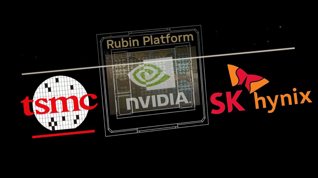
SK Hynix’s strategy is different. As the first-mover in the HBM market, it secured a dominant position by perfecting its mass production techniques and building a trusted relationship with key clients like Nvidia . However, the company lacks a robust in-house foundry for logic dies. For HBM4, SK Hynix made a strategic choice to outsource the production of these critical base dies to TSMC, the world’s dominant foundry . While this leverages TSMC’s advanced process technology, it also introduces significant risks.
This “foundry outsourcing structure” means SK Hynix must align its design to TSMC’s platform, which can reduce the efficiency of integrated design . Furthermore, it forces a more conservative approach to DRAM selection. To ensure production yield stability, SK Hynix initially applied its existing 1b (fifth-generation) DRAM to HBM4, rather than immediately jumping to the newer 1c process like Samsung . While this minimizes early-stage production hiccups, it also means their initial HBM4 products may lag in power efficiency and density. This dependency creates a precarious situation where product supply depends on securing production slots at TSMC, which are also highly sought after by major tech companies .
Technological Deep Dive: The 1c vs. 1b DRAM Divide
The choice between using 1c and 1b DRAM is not a minor technicality; it is central to the performance gap between the two competitors’ HBM4 offerings.
Samsung’s Leap with 1c DRAM:
Samsung’s decision to utilize its sixth-generation 1c DRAM for HBM4 is a bold move that underscores its confidence in its internal capabilities. The 1c process offers far superior density and power efficiency compared to the previous generation . In the world of AI data centers, where power consumption and heat generation (thermal dissipation) are the primary constraints, these improvements are non-negotiable . By using 1c DRAM, Samsung’s HBM4 can achieve the ultra-high speeds of 13 Gbps and beyond that Nvidia demands, while managing heat more effectively . The smaller chip area also increases the number of usable chips per wafer (net dies), giving Samsung a potential edge in cost competitiveness and profitability .
SK Hynix’s Conservative Path with 1b DRAM:
In contrast, SK Hynix’s initial reliance on 1b DRAM is a calculated risk. The 1b process, while mature and reliable, is reaching a physical ceiling for achieving the highest speeds with acceptable power and thermal characteristics . Because SK Hynix cannot directly control the logic die design and thermal structures (which are handled by TSMC), pushing the 1b-based HBM4 to higher performance levels could lead to sharp increases in heat and potential product instability . This conservative approach prioritizes stable initial production yields but could leave them at a performance disadvantage against Samsung’s more aggressive 1c-based design.
Financial Performance: A Changing of the Guard?
The technological race has been mirrored by a fascinating shift in financial fortunes. For decades, Samsung Electronics has been the undisputed financial leader among South Korean chipmakers. However, the AI boom, fueled by demand for HBM, has allowed SK Hynix to achieve a remarkable feat.
In 2025, riding the wave of explosive AI infrastructure investment, SK Hynix reported record-breaking annual results. The company posted an operating profit of 47.2 trillion won ($33 billion) , beating Samsung Electronics’ total performance for the first time in its history . SK Hynix’s revenue for the year jumped 47% to KRW 97.1 trillion ($68 billion) . This demonstrates how a focused strategy on a high-growth, high-value-added product like HBM can propel a company to new financial heights.
Samsung, however, is far from being left behind. While its total operating profit was lower, its memory business remained a powerhouse. Samsung recorded its highest quarterly operating profit in Q4 2025, at KRW 20.1 trillion ($14 billion), with memory revenue hitting KRW 44 trillion ($31 billion) . This robust financial health provides Samsung with the capital to invest aggressively in regaining its leadership position. Both companies plan to significantly increase capital expenditure (capex) in 2026 to expand production capacity for HBM and other advanced chips, signaling a long-term commitment to dominating the AI memory market .
Market Share and Future Outlook: Who Will Prevail?
The battle lines for market share in HBM4 are being drawn now, with analysts offering differing projections based on the latest developments.
A. Current Market Projections
Initial estimates from firms like Counterpoint Research suggested SK Hynix would maintain a commanding lead, projecting a 54% share of the global HBM4 market in 2026, followed by Samsung at 28% . However, more recent analysis suggests the race is tightening considerably. Following Samsung’s successful mass production announcement and reports of Micron’s failure to meet Nvidia’s HBM4 speed requirements, the market is now expected to be a two-way duopoly between the Korean giants . Some analysts now predict SK Hynix could secure around 70% of Nvidia’s initial HBM4 orders, with Samsung taking the remaining 30%, though this split is highly dynamic and subject to change based on performance validation and yields .
B. Future Roadmaps: Custom HBM and Hybrid Bonding
Looking beyond HBM4, both companies are plotting their courses for future generations, including HBM4E and HBM5.
-
Samsung’s Roadmap: Samsung has unveiled an ambitious plan to develop customized HBM chips that it claims can deliver up to 2.8 times higher performance than its current HBM4 . The company is already looking toward HBM4E sampling in the second half of 2026 and is investing in next-generation technologies like hybrid bonding. This new method, which eliminates the bumps used in current TSV technology, is essential for stacking more than 20 layers of memory dies within the strict height limits of processor packages .
-
SK Hynix’s Roadmap: SK Hynix is not resting on its laurels. The company has introduced its “HBM BTS” strategy, which aims to offer specialized HBM solutions optimized for different customer needs: Bandwidth (B), Thermal Dissipation (T), and Space Efficiency (S) . This acknowledges that AI accelerators are becoming more diverse, requiring tailored memory solutions rather than a one-size-fits-all product. Like Samsung, SK Hynix also acknowledges that hybrid bonding will be crucial for ultra-high-stack products exceeding 20 layers and is actively developing the technology .
Broader Implications and Conclusion
The Samsung vs. SK Hynix race is more than a corporate rivalry; it has profound implications for the entire AI ecosystem. Their intense competition accelerates the pace of innovation, leading to faster, more efficient memory that enables the next generation of AI models. For the global supply chain, their dominance now essentially a duopoly in the HBM4 market creates both stability and risk . While they are reliable partners for companies like Nvidia, AMD, and Microsoft, it also creates a point of extreme concentration .
Furthermore, the race highlights the shifting dynamics in the semiconductor world. Pure memory prowess is no longer enough; success now requires expertise in logic design, foundry partnerships, and advanced packaging. Samsung’s integrated model offers synergy and speed, while SK Hynix’s specialized approach, bolstered by its partnership with TSMC, offers focus and agility.
In conclusion, the race between Samsung and SK Hynix is far from over. It is a multi-front war spanning technology, finance, and manufacturing strategy. As they push the boundaries of what memory can do transforming it from a simple storage component into an active partner in computation they are not just competing for market share; they are building the very foundation of the AI-driven future.
Frequently Asked Questions (FAQs)
1. What is HBM and why is it important?
High Bandwidth Memory (HBM) is a high-performance memory interface used in AI accelerators and supercomputers. It is important because it provides the immense data transfer speeds needed to feed AI processors, preventing them from stalling while waiting for data.
2. What is the main difference between Samsung and SK Hynix’s HBM4 strategy?
Samsung uses a vertically integrated approach, designing its memory, logic die, and packaging in-house. SK Hynix outsources the production of its logic die to TSMC, allowing it to focus on memory stacking and yield optimization.
3. Who is currently leading the HBM4 race?
As of early 2026, Samsung drew first blood by announcing the mass production and shipment of its HBM4 chips. However, SK Hynix is expected to secure a significant portion of initial orders from Nvidia, making the leadership position highly contested.
4. What are 1b and 1c DRAM?
These are generations of DRAM manufacturing processes. “1c” is the sixth generation, offering better power efficiency and density than the fifth-generation “1b.” Samsung is using 1c for its HBM4, while SK Hynix initially used 1b.
5. What is hybrid bonding?
Hybrid bonding is an advanced chip stacking technology that directly connects copper pads of two dies without the use of “bumps” or solder. It allows for finer interconnections and is essential for stacking more than 20 memory layers in future HBM products like HBM5.


